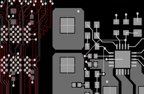
In an electronic CAD Flow it is important that the design intent is captured as much as possible in electronic form. This includes also all kind of design rules. Upcoming issues during the PCB design process shall be addressed as early in the design process as possible to keep the cost of change and redesign low. When all information is stored in the design database, they are also available, when a redesign or design reuse is required later on.
Many design rules are important for Signal Integrity (SI) and Power Integrity (PI) to ensure the functionality of the circuit. Design for manufacturing, reliability, high voltage or high current and test also put design restrictions to the designer as rules. FlowCAD has a lot of knowhow about PCB design and is qualified to sell and support solutions for electronics design to help develop and manufacture optimized electronic.
OrCAD PCB products offer a professional PCB layout solution from Cadence Design Systems at a very reasonable starting price. OrCAD PCB software is scalable as needed and expandable to the Allegro product family on the same database. The PCB Design flow includes OrCAD Capture for schematic entry and a constraint manager to drive real time design rule checks (DRC). It is capable to easily and efficient PCBs with i.e. DDR3 memory and differential pairs as well as power supplies.
More
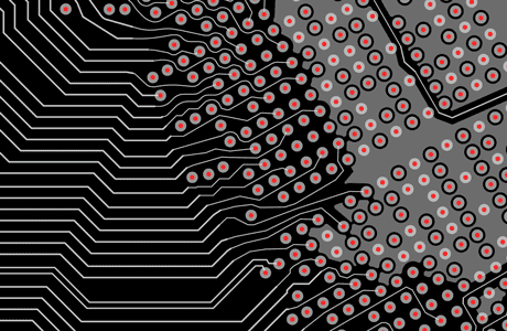
The Allegro PCB Design flow is the higher performance part of the scalable PCB layout solution from Cadence. It enables users to run signal and power integrity checks and simulations directly in the PCB tool. In an engineering team users can work in parallel for small projects or complex systems on one circuit schematic or a PCB layout together. Direct flawless integration for SI, PI and RF of Cadence simulation tools enable highest accuracy of virtual measurements. Today the most complex electronic designs are made with Allegro PCB Designer.
More
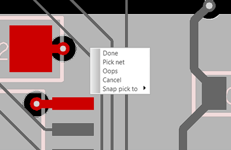
FloWare Modules are part of a toolbox to enhance productivity for OrCAD PCB Editor and Allegro PCB Editor.
These modules are made to increase efficiency for specific tasks, which might not be used by all customers in a standard flow.
FloWare offers solutions for additional checks, manufacturing options, added SI features, documentation, and more.
Menu structures are automatically recognized by PCB Editor and shown in the tool bar.
More
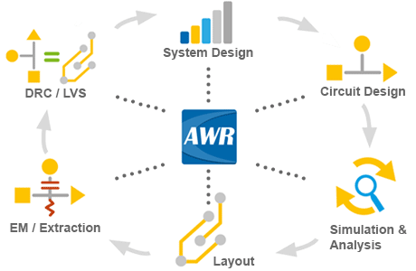
To support increasing functionality, printed circuit boards employ more complex board structures designed for a range of specialized applications. Offering a layout-driven design methodology for complex RF PCBs, AWR Design Environment supports accurate modeling of PCB transmission media from the RF signal path to digital control and DC bias lines. Circuit / system and electromagnetic co-simulation provides first-pass design success with complete PCB analysis of surface-mount components, interconnecting transmission lines, embedded and distributed passive elements, as well as EM verification.
More about AWR
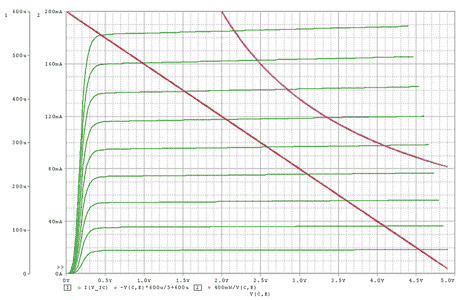
Even experienced electronics developers can hardly predict the behavior of electrical circuits. Therefore, circuits, whole systems or only critical circuit parts are analyzed either by physically constructed prototypes and subsequent measurements or by circuit simulations. The trend here is clearly towards virtually simulated measurement, as the development cycles are getting shorter and shorter, and simulations can be used very promptly to make statements that correlate with measurements. Worldwide, PSpice has been the reference simulator for years, and most component manufacturers offer PSpice simulation models on the Internet.
Learn more
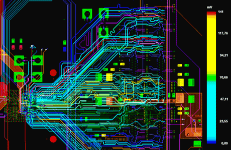
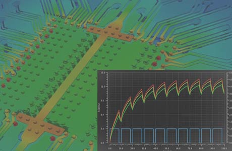
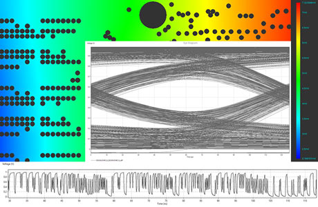
For Cadence users, Sigrity technology has been consolidated into deep integrated simulation and is offered as a scalable Allegro Sigrity solution. Essentially, the Sigrity methodology is divided into two categories, the analysis of the power supply system (power integrity - PI) and the signal integrity (SI), taking into account fluctuations in the power and voltage supply. Simulations can be done separately or in the background in the Allegro PCB Editor.
Learn more
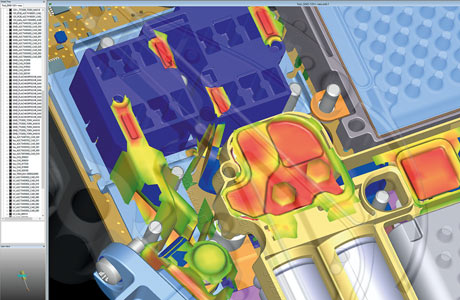
Thermal Simulation seamlessly integrates with Cadence IC, package, and Allegro PCB platforms.
Fast and accurate parallel simulation enables new system analysis and design insights and empowers electrical design teams to detect and mitigate thermal issues early in the design process - reducing electronic system development iterations. Engineers can combine PSpice, Celsius and Sigrity in an accurate electrical and thermal co-simulation (steady-state and transient) system-level thermal simulation for PCB and IC-Packaging based on the actual flow of electrical power.
Solving Thermal Problems
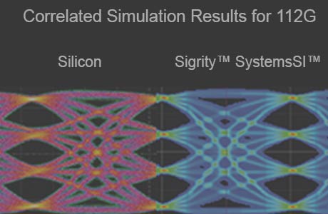
Clarity 3D Solver is a true full wave 3D electromagnetic (EM) simulation software tool for designing critical interconnects for PCBs, IC packages, and system on IC (SoIC) designs. Clarity 3D Solver resolve the most complex electromagnetic (EM) challenges when designing systems for 5G, wifi-6, high-performance computing (HPC), and machine learning applications with gold-standard accuracy. This multiprocessing technology enables to deliver virtually unlimited capacity and 10X speed required to efficiently and effectively address these larger and more complex structures. It creates highly accurate S-parameter models for use in SI, PI, and EMC analysis, enabling simulation results that match lab measurement, even at 112Gbps+ data transfer speeds.
Datensheet Clarity 3D Solver
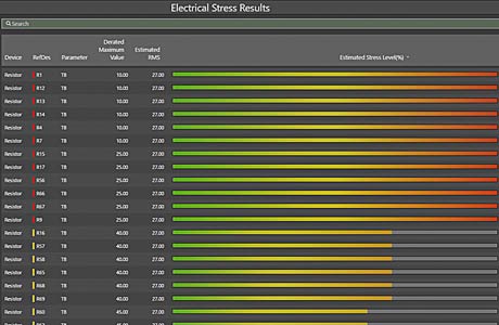
In a schematic audit you can verify with 30+ rules the integrity of your schematic for net-connectivity, part-properties and component-values and cross-probe to instances and nets to fix warnings and errors. Electrical overstress analysis based just on the schematic verifies electrical stress for each device in the design and visualize stress reports with different derating. With schematic ERC basic connectivity checks are performed for schematic grammatic correctness.
More
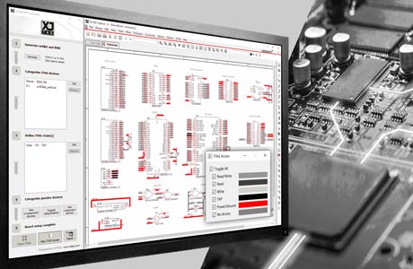
XJTAG's Boundary Scan solution provides a cost-effective way to prepare and create Boundary Scan test protocols. In conjunction with the schematic entry tools from Allegro, Altium, OrCAD, Siemens/Mentor and Zuken you successfully perform boundary scan test preparation and see test coverage in the schematic tool.
More
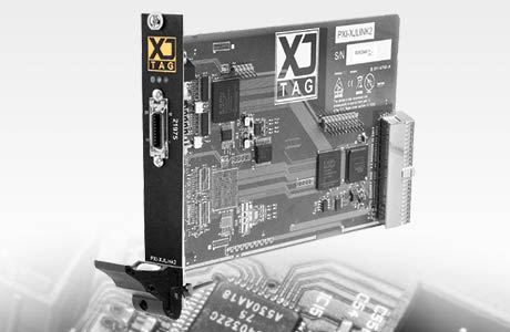
XJTAG's Boundary Scan test solution include in delivery a case with all the hardware and software needed to successfully perform boundary scan tests. The USB interface adapter XJLink or XJLink2 is used to establish the connection between the PC and the JTAG interface on the prototype circuit board.
More
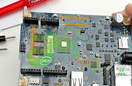
inspectAR is an intelligent PCB viewer that displays the PCB together with the design data as an augmented reality overlay in real time. The live image of the PCB is captured via webcam or mobile phone. The software recognizes the PCB dimensions and compares the coordinates with the design. With inspectAR, enormous time can be saved when bring up prototypes, during troubleshooting and repair or in quality assurance.
More
Creepage and clearance analysis in NEXTRA is based on the ability to exactly or approximately calculate the distances between powered elements within an electro-mechanical design database. Creepage is thus defined as paths on the surface of insulators between two powered elements. Clearance however is the path through air between two powered elements. Relevant parameters that impact creepage and clearance violations are mostly identified and characterised in various standards, e.g. DIN EN 60664 (IEC 60664-1) in Europe, Germany or world-wide, respectively their sub-norms.
NEXTRA datasheet
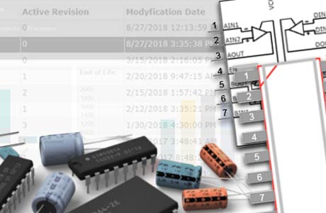
Electronic Design is more than a schematic and a PCB layout. Price, availability, product change notifications, certifications and more external data have an influence on the decisions, which components an engineer can select for the design. The speed how fast these information about electronic components are changing over their lifetime is increasing and might even change during the development process. Electronic Data Management (EDM) solutions help getting and maintaining this meta data of electronic components.
More
PCB design tools place symbols and footprints from a component library. Library quality has direct impact on the quality of the designs. Building and maintaining a good library is not so easy, because components can become obsolete, similar components are available from multiple vendors and production processes from two fabricators might require different geometries and rules for pads and footprints. Multiple solutions are available from different vendors. Which tool or solution suits your needs best is different from user to user.
More
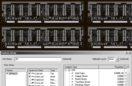
WISE specializes in preparing, displaying and validating CAM data. Many users want to check the manufacturing data of their PCB layout software in a third-party vendor independent tool before the data is used for production. WISE has become known through the GerbTool, but today is also very committed to the IPC consortium to support and validate the new IPC 2581 standard.
GerbTool datasheet
FlowCAD's PCB layout services can expand your bandwidth. We can create your PCB layout on OrCAD, Allegro or other layout systems. Our experienced PCB designer are familiar with multiple layout systems as well as multiple industry requirements. We can be on site within your facilities and work in your network or you transfer the data to us and we work from our office in Feldkirchen close to Munich. The difference between these two models is just the travel cost. Our broad expertise covers applications like automotive, industrial automation, high current, high speed (SI / PI), telecom and IC-tester boards.
Learn more
FlowCAD's simulation services can help you to perform electronic simulations. We support circuit simulations with PSpice, signal integrity, power integrity, thermal analysis, analysis of creepage and air gaps with the tools from Cadence. We can help you build a simulation model library or run certain simulations for you. When purchasing your own simulation tool we can work on the first simulation projects after your training together to enable a fast learning curve.
Learn more