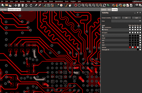
Conception de PCB en 3D avec fonctions d'édition

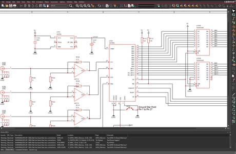
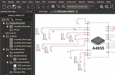
Schéma de circuit et recherche de composants en ligne

L'outil de conception de PCB à la pointe de la technique

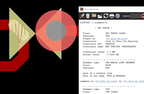
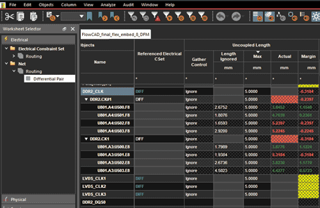
Gestion globale des contraintes

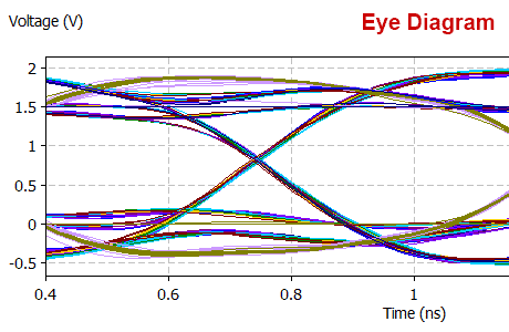
Simulation de l'intégrité du signal
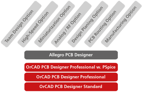
OrCAD PCB Designer Standard (Work from Home)
Pendant ce temps, les développements électroniques ont lieu complètement ou temporairement dans le bureau à domicile. L'accès aux licences logicielles à domicile est un problème pour de nombreuses entreprises.
Pour faciliter le travail à domicile, FlowCAD et Cadence ont lancé le programme de travail à domicile. Nous offrons la licence d'achat du "OrCAD PCB Designer Standard" y compris 2 ans de maintenance, pour un prix spécial de EUR 999.00 !
€ 999.00 prix net
y compris 2 ans de maintenance
Livraison dans les délais :
3-4 jours ouvrables
En stock.
Prix régulier :
€ 2'630.00 y compris 1 an de maintenance
hors TVA
Veuillez noter que :
Dernière date de réception des commandes : 20 septembre 2023
Vente et livraison par FlowCAD Schweiz AG. La facture peut être convertie en francs suisses au taux de change du jour.
Il n'y a pas de droit de retour pour les logiciels commerciaux, veuillez d'abord utiliser la version gratuite TRIAL. Vente en ligne uniquement aux entreprises.