Profesjonalny projekt płytki drukowanej, układ płytki i prowadzenie
Silnik Allegro w OrCAD wspiera Twoją produktywność. OrCAD oferuje układ PCB, szybki routing i opinie elektroniczne w czasie rzeczywistym, aby pomóc Ci szybciej przygotować projekt PCB.
Placement
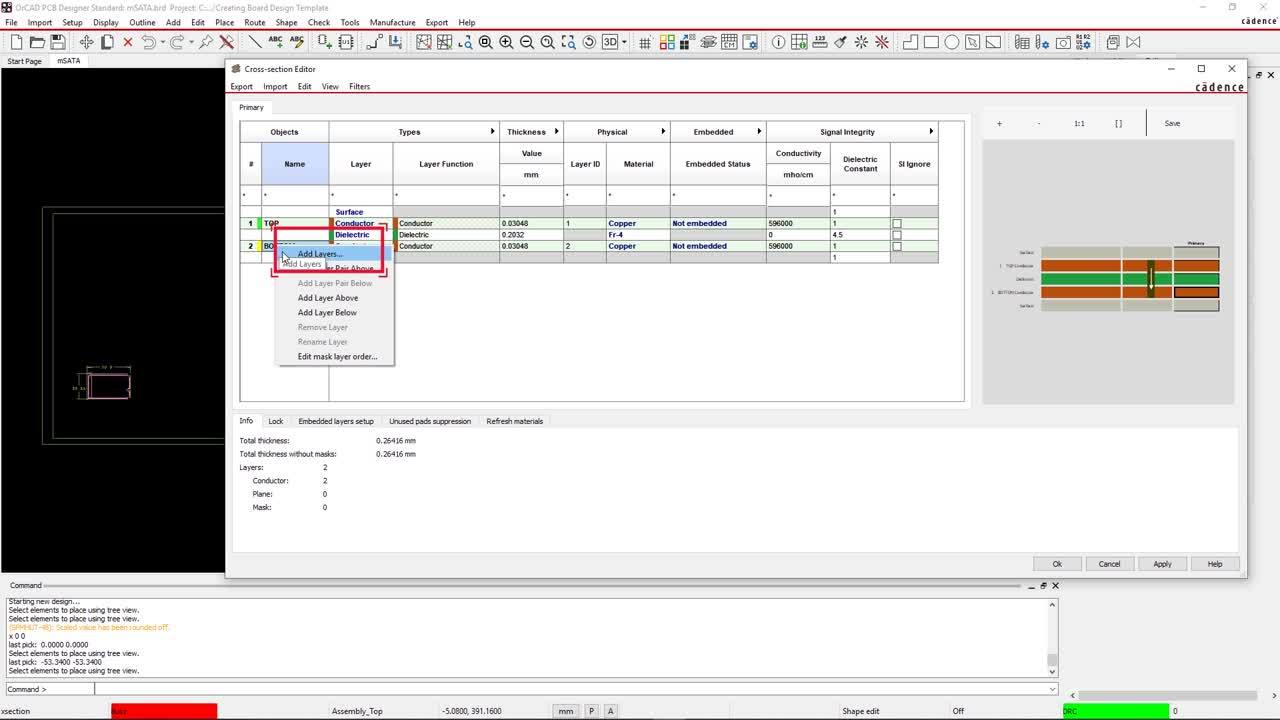
Board Outline and Dimensioning
Use templates to assist with the board outline, drawing format, and basic design rules.
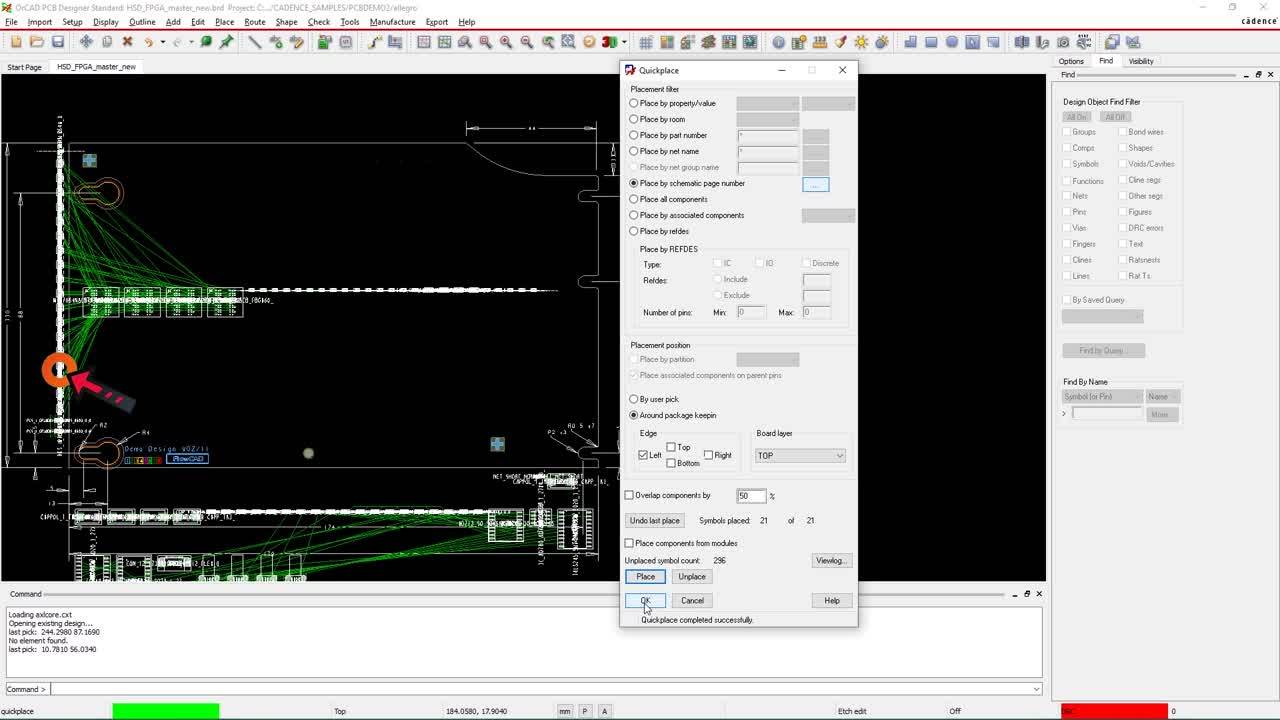
Component Placement
Arrange the symbols for your circuits in groups according to schematic environment.
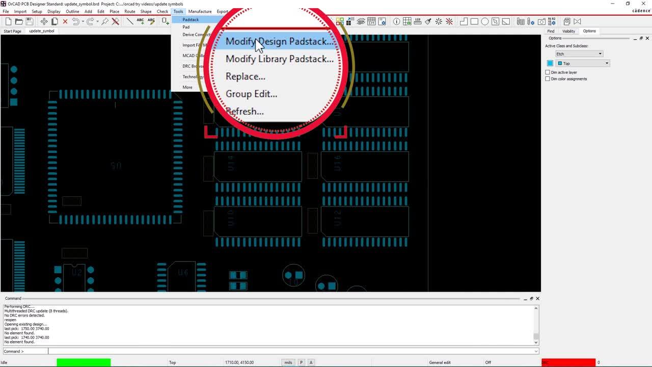
Symbol Update in PCB Layout
Revise symbols and modify design padstacks.
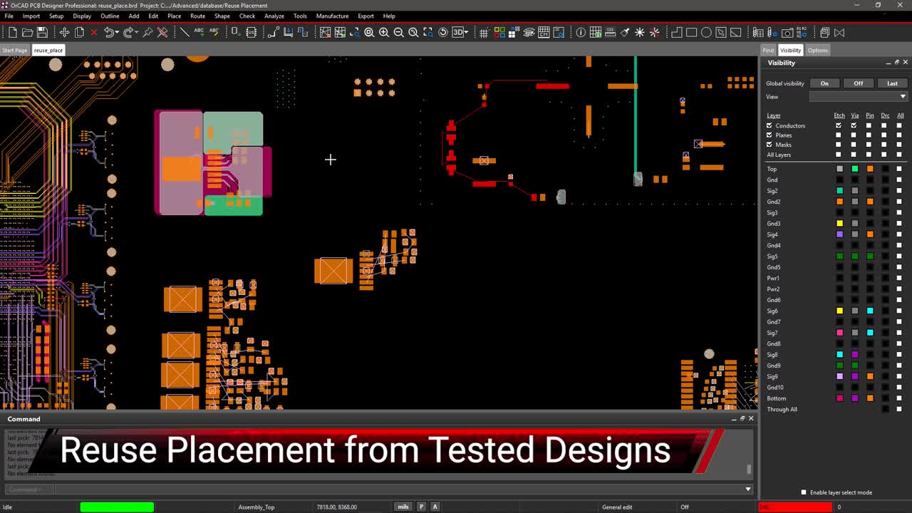
Reuse Placement from Tested Designs
Save time by reusing known good design with similar placement and routing without needing to reinvent the wheel.
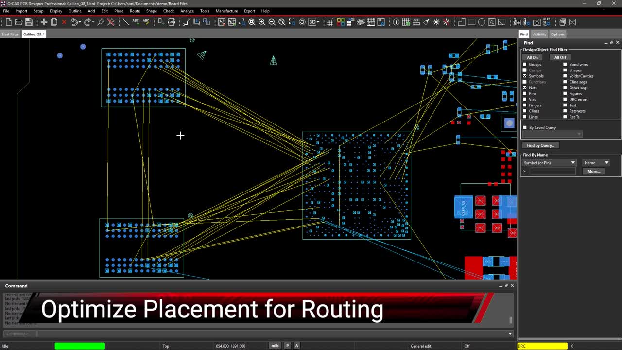
Optimize Placement for Routing
Place components based on your own design rules with color coded indicators to keep check on placement.
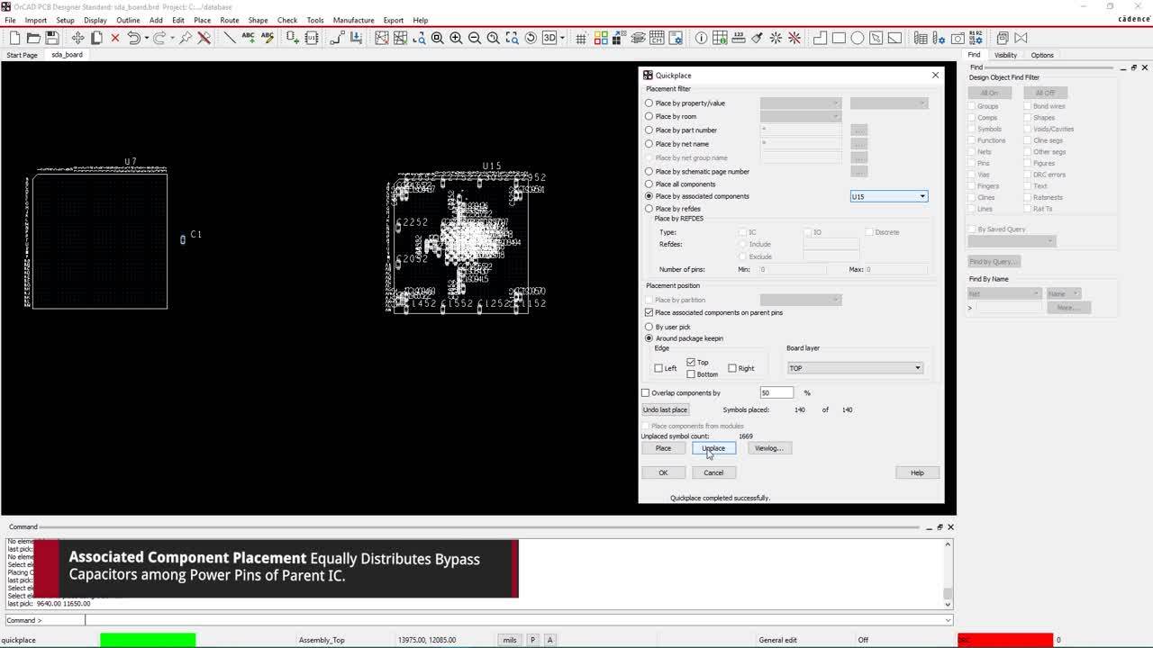
Bypass Capacitor Placement
Position Bypass Capacitors within the required distance from power pin of IC.
Design Rules
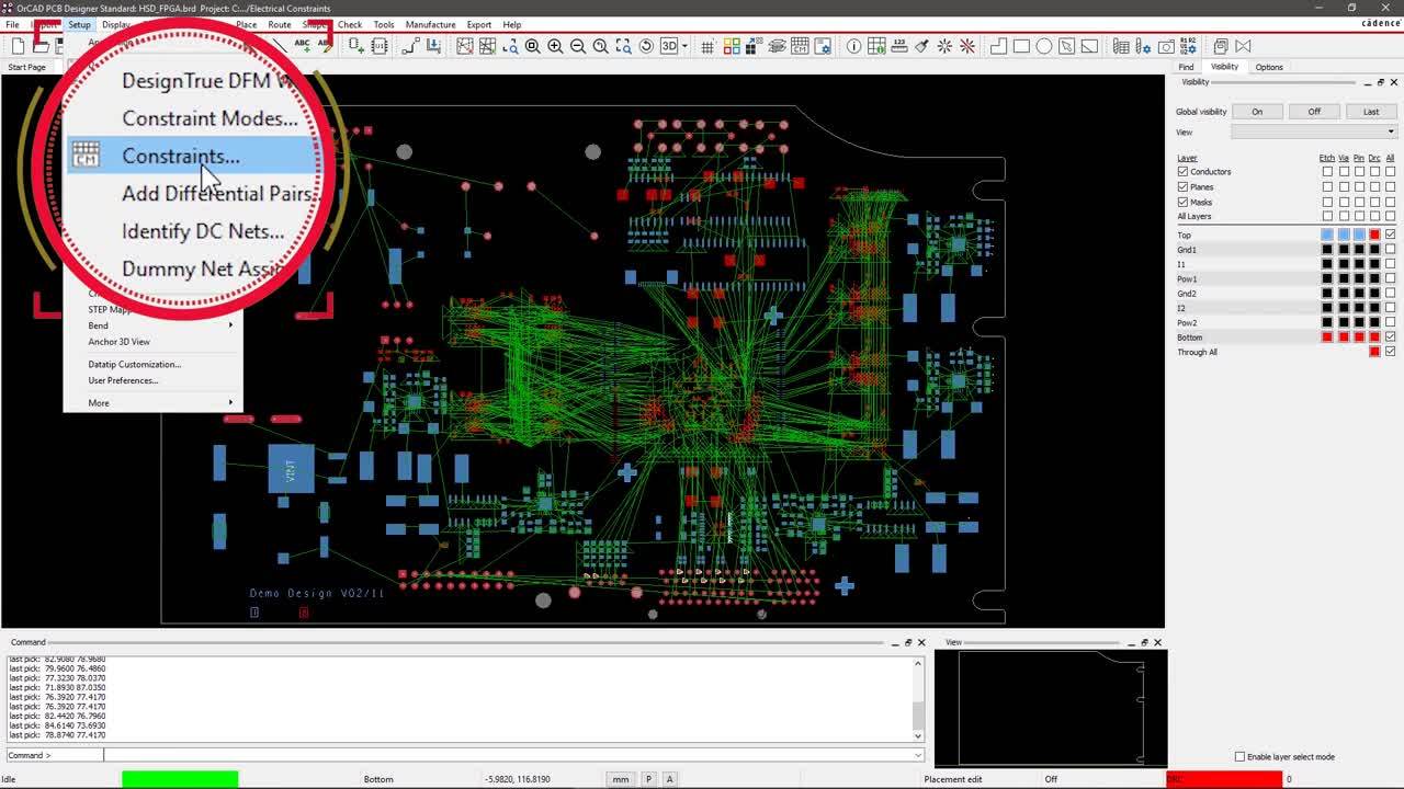
Electrical Design Rules
Apply and analyze constraints for making electrical connections between components.
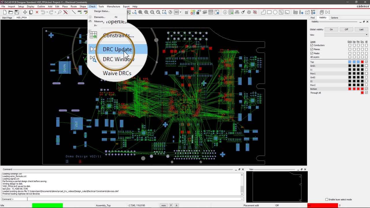
Physical Design Rules
Define physical parameters like spacing, line widths and vias.
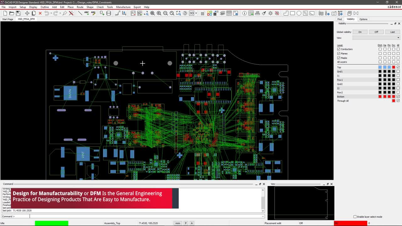
Design for Manufacturability
Setup constraints to make your PCB good enough for fabrication, assembly and testing.
Routing
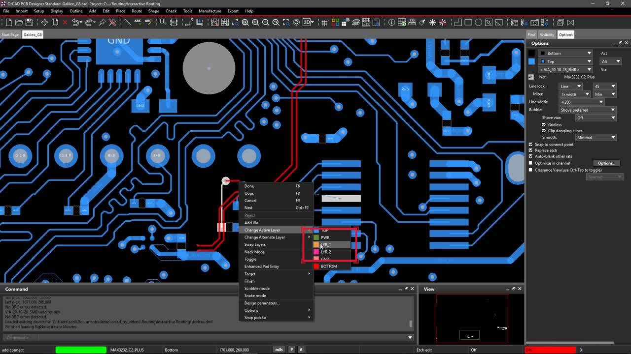
Interactive Routing
Draw and edit connections between pins or pads after placement.
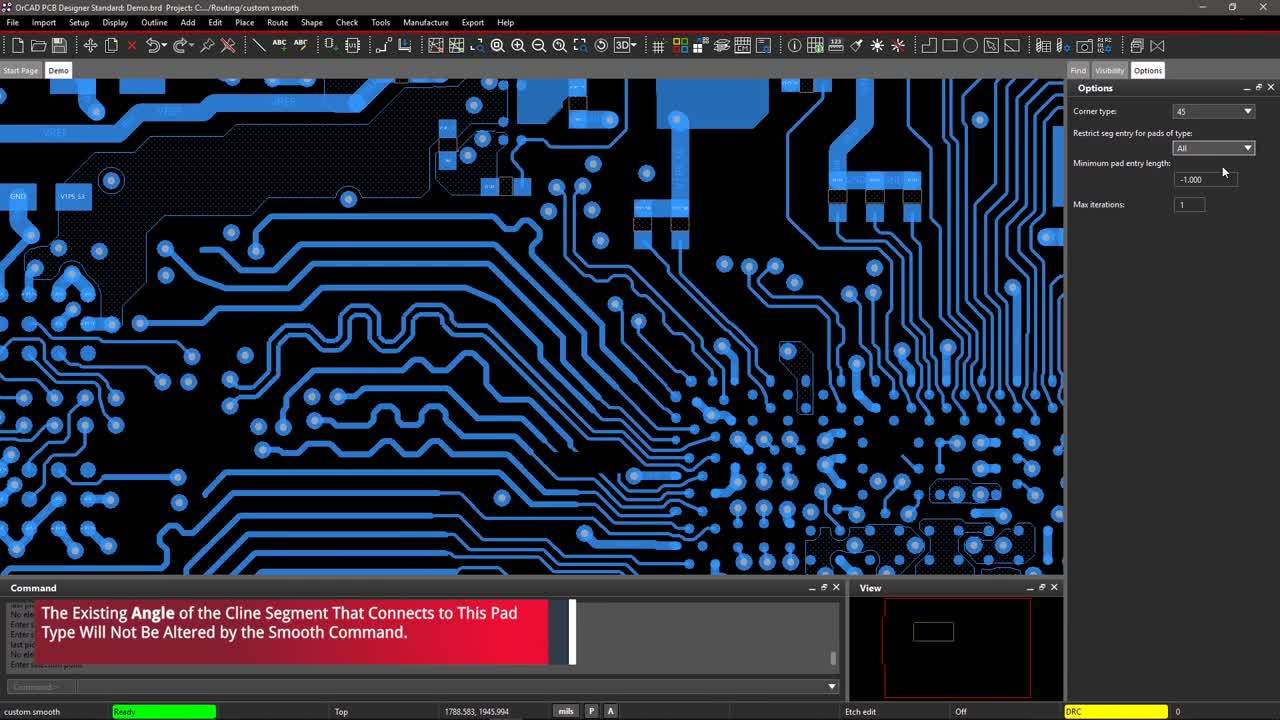
Transmission Line Smoothening
Minimize the distance to pin or pad connections using the custom smooth.
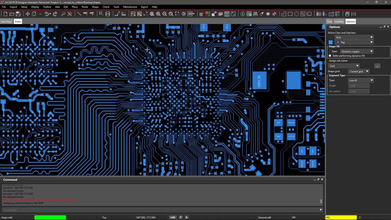
Creating Reference Planes
Add ground and power planes to different layers in your design.
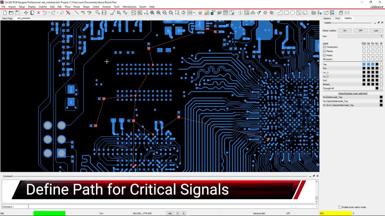
Define Path for Critical Signals
Easily define topology for the critical signals in your design using the Net scheduling command.
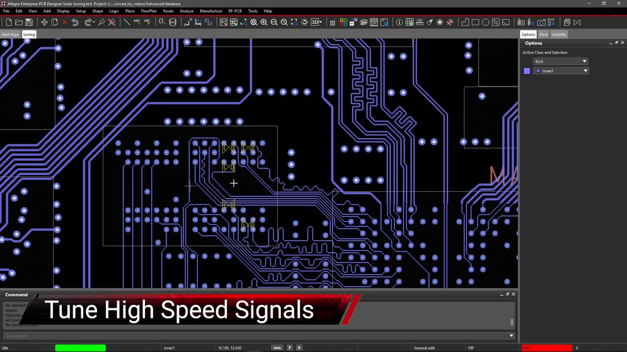
Tune High-Speed Signals
Easily route differential pairs from transmitter to receiver while adjusting phase and time for signal integrity.
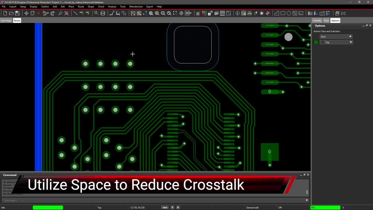
Utilize Space to Reduce Crosstalk
Utilize leftover space on your board by distributing transmission lines evenly reducing crosstalk in routing signals.
Proofing
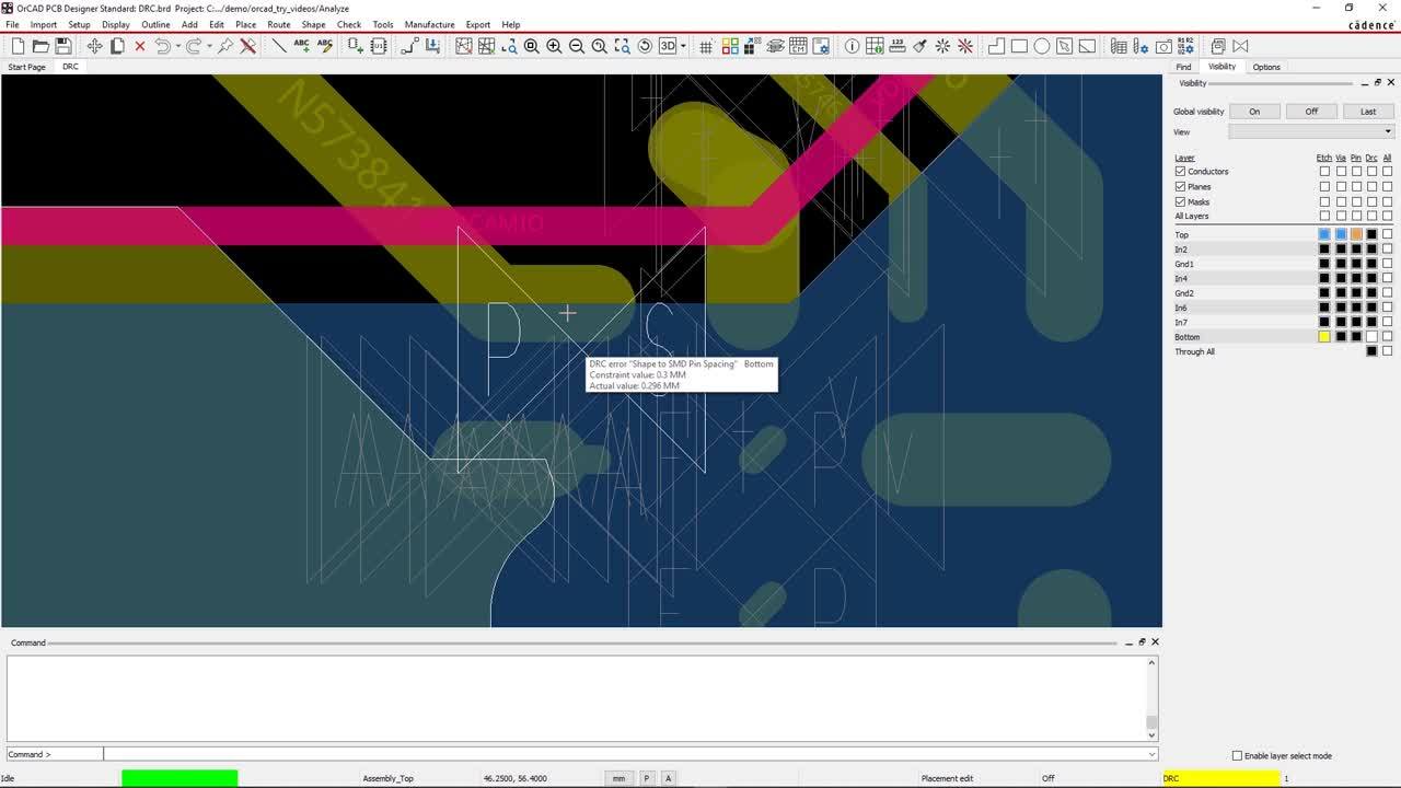
Design Rule Verification
Shorten the design cycle by fixing DRC violations earlier with the DRC browser.
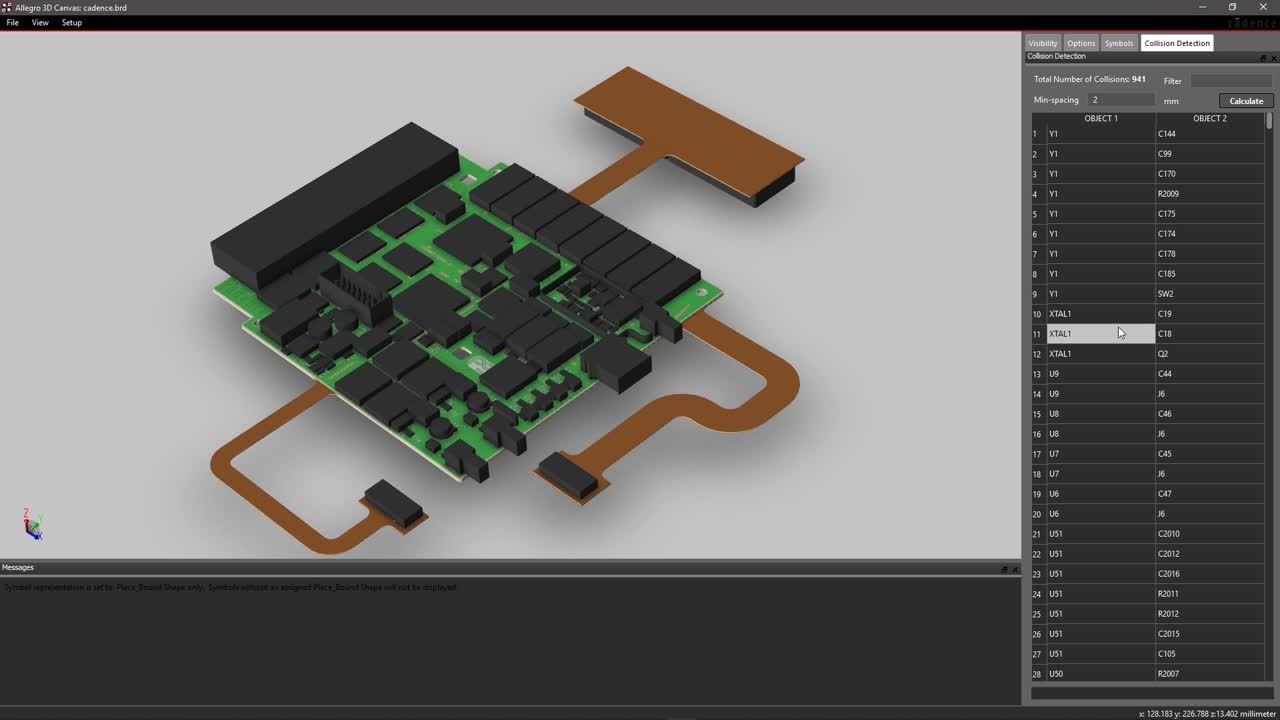
Visualization of your Design
Analyze a three-dimensional model of a design as manufactured output.
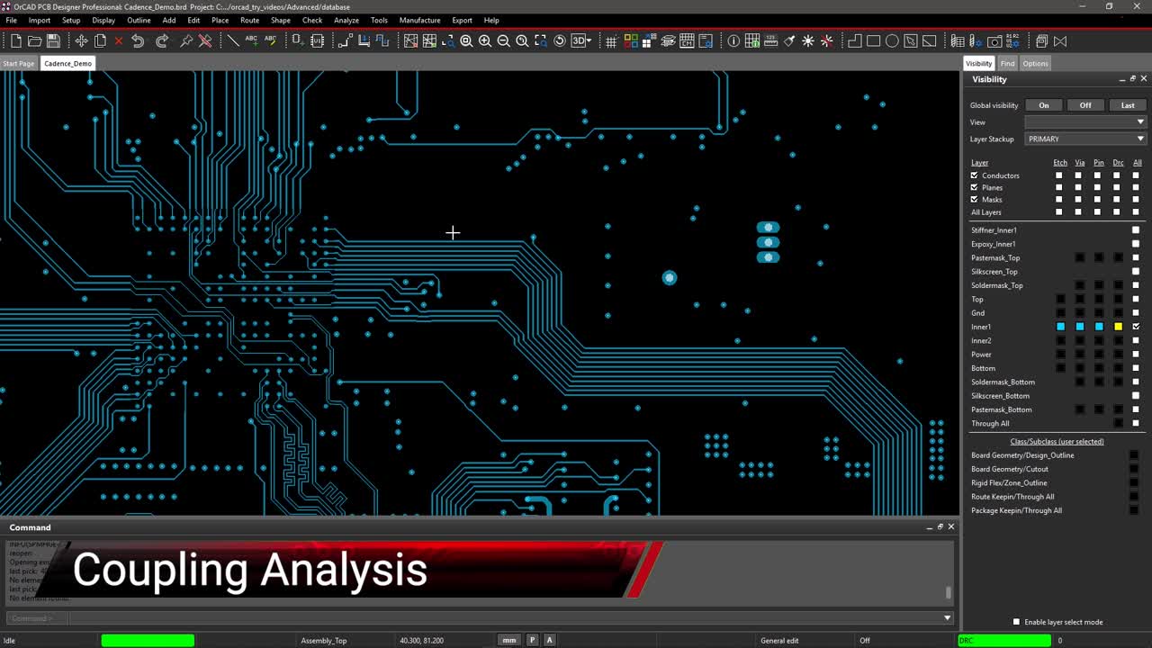
Coupling Analysis
Inspect your traces to resolve any coupling issues due to position of the routes.
Manufacturing
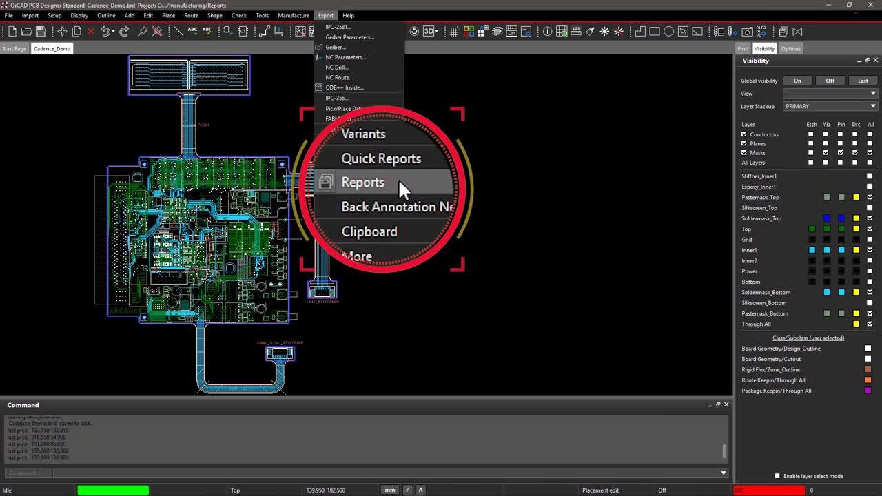
PCB Design Reports
Generate various database reports from your design.
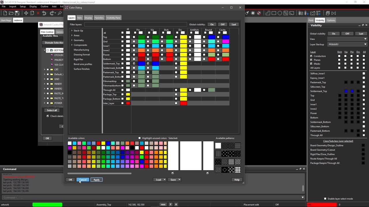
Gerber Generation
Generate layer films from your design to use for manufacturing.
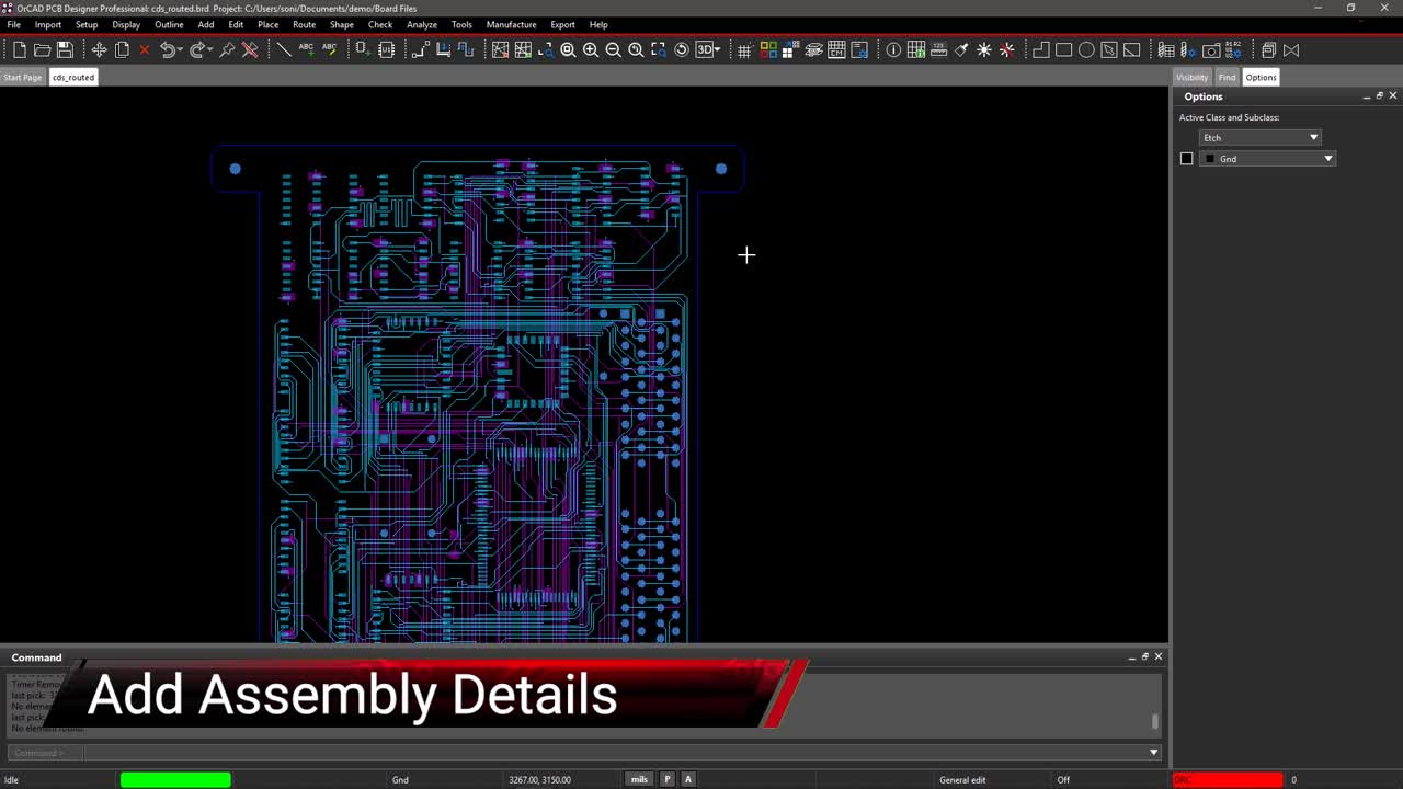
Add Assembly Details
Easily use OrCAD Documentation to add component placement and mounting notes for the fabrication house.
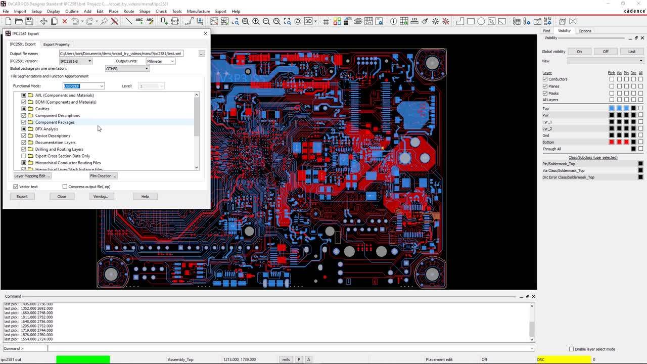
IPC-2581 Compliant Data
Accurately combine all the necessary details into a single file for fabrication.
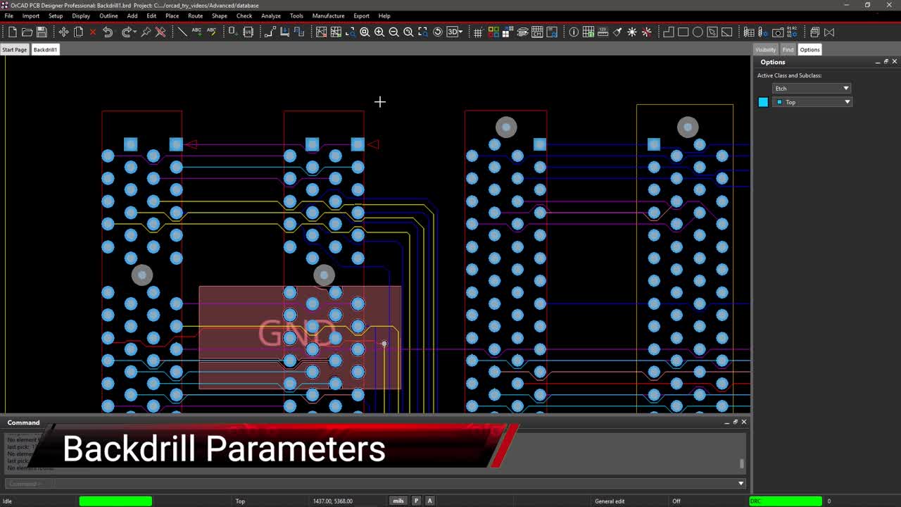
Backdrill Parameters
Generate manufacturable backdrill data for removing stubs and improving signal integrity with blind and buried vias.
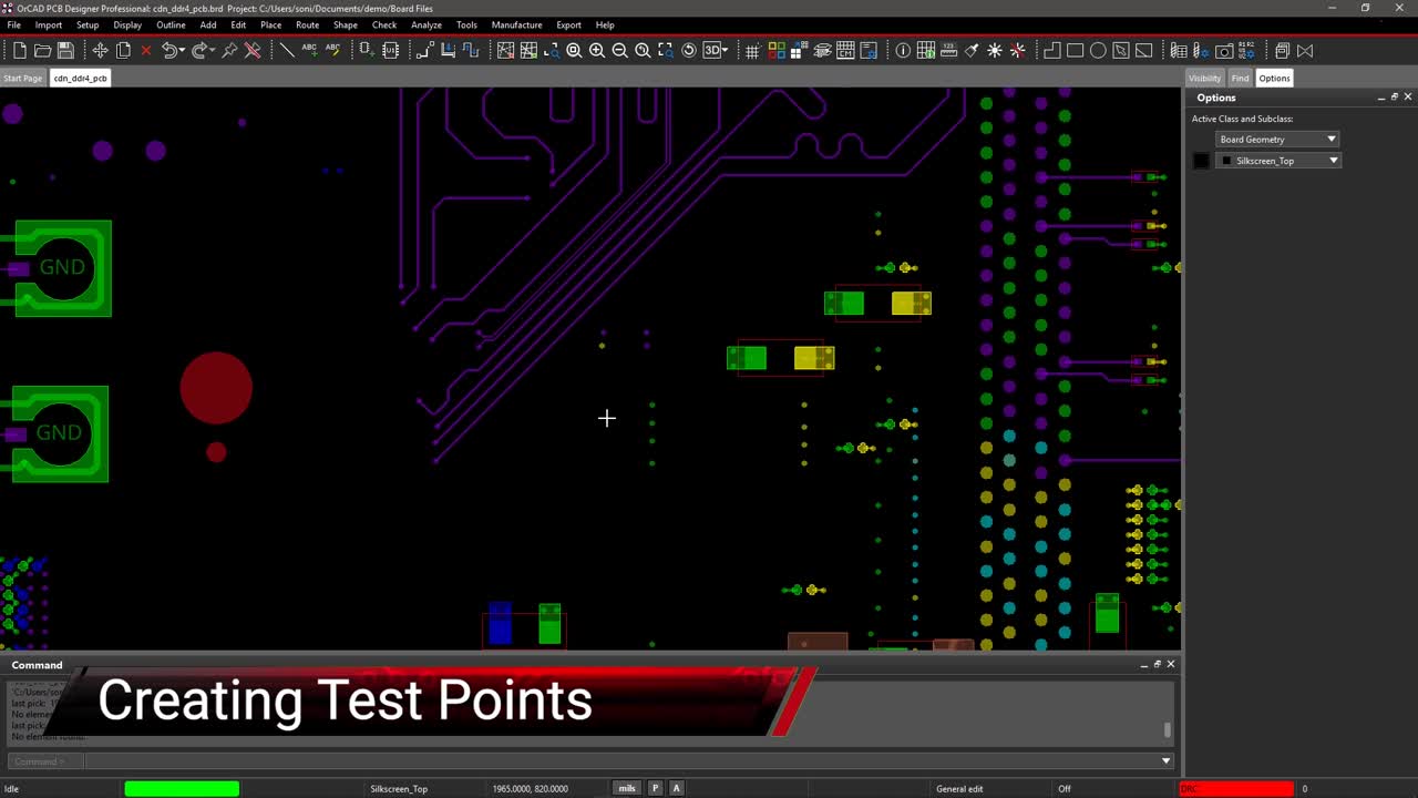
Creating Test Points
Monitor the state of circuitry with BBT and ICT checking for shorts, opens, capacitance, resistance and more.
Rigid Flex
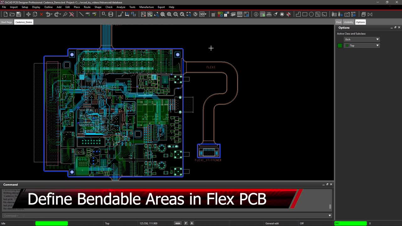
Define Bendable Areas in Your Flex PCB
Define the bend angles for rigid flex and make connections within different cross sections.
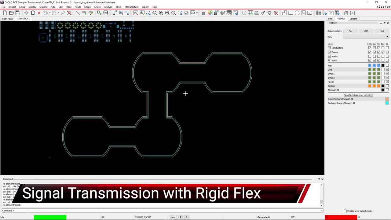
Signal Transmission with Rigid Flex
Select the right materials and layer stackup for the rigid flex areas in your board.