Sigrity Aurora

Sigrity Aurora

Cadence Sigrity Aurora provides traditional signal and power integrity (SI / PI) analysis for pre-layout, in-design, and post-layout PCB designs. Integrated with Cadence OrCAD and Allegro PCB editing and routing technologies, Sigrity Aurora users can start analyzing early in the design cycle using “what if” exploration scenarios in order to set more accurate design constraints and reduce design iterations. Power Feasibility Editor helps to select the right combination of decoupling capacitors in pre-layout.

Sigrity Aurora reads and writes directly to the Allegro PCB database for fast and accurate integration of design and analysis results. It provides a SPICE-based simulator and the patented Sigrity embedded hybrid field solvers for extraction of 2D and 3D structures. It supports power-aware default model library, IBIS (behavioral) models, as well as transistor-level models, if necessary. High-speed signals can be explored pre-layout, to compare alternatives, or post-layout, for a comprehensive analysis of all associated signals.

Key Benefits
  • Detects SI and PI design errors early to reduce design re-spins and increase first-pass success
  • Explores alternative topologies in the earliest stages
  • In-design analysis provides guidelines to minimize EMI already during PCB layout phase, specifically created for PCB designers
Features
  • Tightly integrates Sigrity analysis engines with OrCAD and Allegro PCB Editor
  • Provides quick screening of a design for SI problems without the need for SI models
  • What-if topology circuit simulation using the modern Allegro system capture canvas
  • Provides in-design SI / PI analysis within a constraint-driven flow
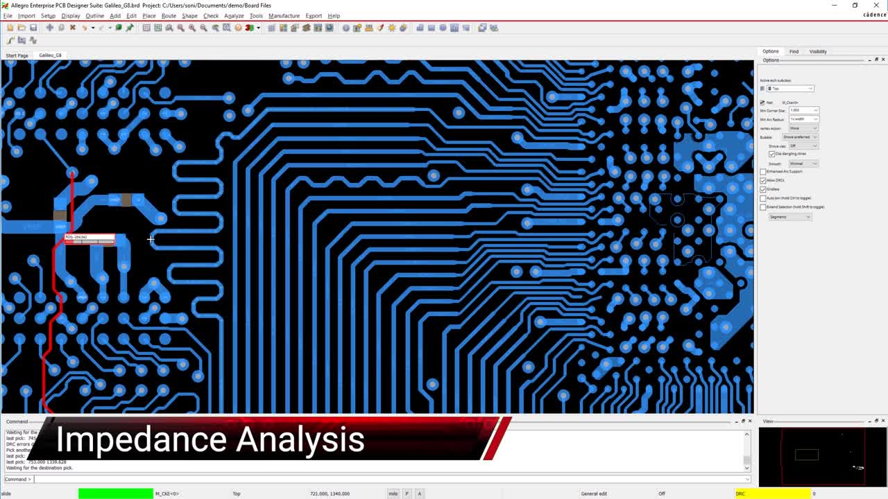
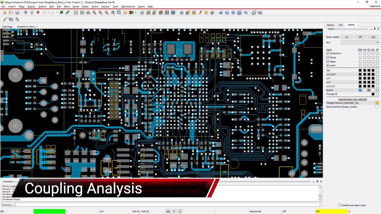
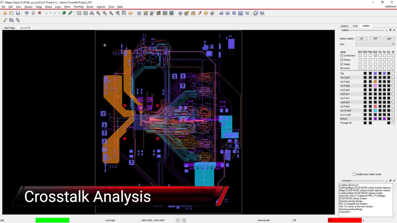
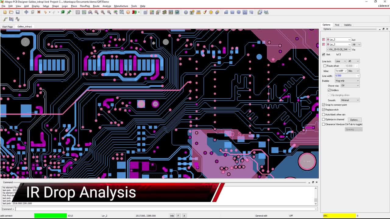
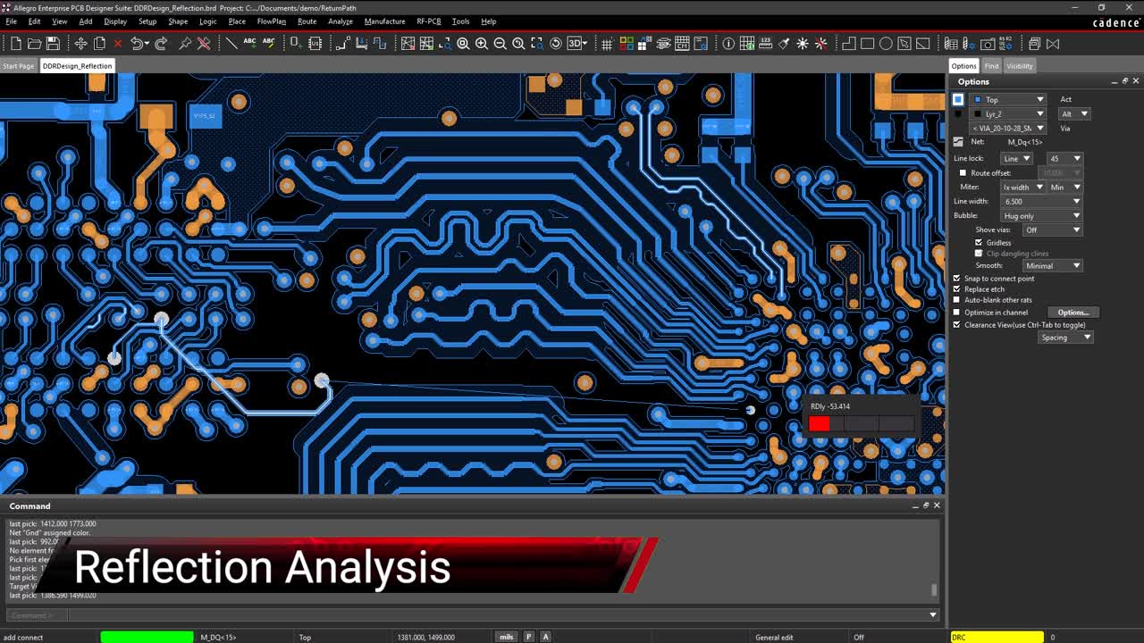
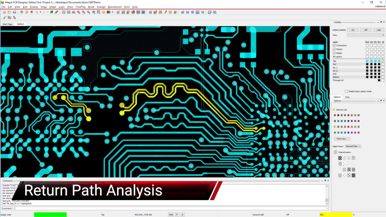
  • Impedance discontinuities, coupling, crosstalk, reflections, IR-drop, and return path analysis
  • Support of live Allegro PCB Symphony Team Design session to perform SI / PI analysis without making a copy of the design
Pre Layout
In-Design
Post Layout
Workflow Videos
Aurora is the Pre and Post Layout Simulation Tool and In-design Analysis (IDA) in PCB Editor

Pre-Layout Analysis

What if Exploration
What if Exploration

“What if” Exploration

Sigrity Aurora users can start analyzing early in the design cycle using scenarios in order to set more accurate design constraints and reduce design iterations. User can explore alternative topologies, track length, reflections and different impedances in the earliest stage based on a schematic and a PCB stackup. What-if topology circuit simulation is using the modern Allegro system capture canvas to verify constraints.

In-design Analysis Workflows

In-design analysis (IDA) workflows will work with OrCAD and Allegro PCB Editor. The workflows help the PCB designer, like a spell checker in MS-Word, to run quickly standardized simulations in the background, while he is routing the PCB layout. The workflows are providing immediate feedback if a variation of a layout is getting better or worse. This helps the designer to create electrically better geometries at the earliest stage and avoid complicated changes or redesigns later in the development process.

The current of fast switching signals in high-speed signals will generate electromagnetic fields which have an influence on conductors in the surrounding. Miniaturization with smaller spacing, higher frequencies and lower supply voltages with small tolerances increase this effect. PCB designers have to make compromises to balance the effects like radiated EMI noise which cause failure in FCC testing, size of the board, thermal issues and cost. 3D field solvers can simulate and visualize the electromagnetic fields in a PCB. Visualization of hotspots guides the PCB designer to reduce the noise level and improve signal integrity (SI), power integrity (PI), and electromagnetic interference (EMI).


Impedance IDA Workflow
Impedance IDA

Impedance IDA

The impedance workflow checks the PCB layout data consisting of layer stackup and the lines, vias and areas on each layer, where there are jumps or discontinuities in the impedance. At places where e.g. a signal line has an interruption in the reference layer for the return current, the impedance changes. These areas are colored differently. In this way, PCB designers can identify the critical points in the layout, where reflections occur on the signal lines that are the cause of poor signal quality or EMC interference.

Reflection IDA Workflow
Reflection IDA

Reflection IDA

The workflow for reflection will use either default models like "10 Ohms, 3pF, 2,5V" or real IBIS models. Once the models are assigned, the PCB designer can run these simulations to see the Rx and Tx wave forms for receiver and transmitter. Changes in the layout will change the wave form and the designer can improve his layout when the curves for i.e. overshoot, monotony and delay are getting better. Small changes early in the design process have a positive impact on signal integrity (SI) and EMI. The fast feedback of layout geometry and waveforms is unique with Cadence PCB Design.

Coupling IDA Workflow
Coupling IDA

Coupling IDA

When two traces are routed in parallel the signals might couple and interfere. Critical nets should not couple and it is an important information for the PCB Designer, to see where traces are coupled. This is a physical feedback about the length and distance of two traces to each other. Colored traces show where coupling is high and the PCB designer wants to improve, if possible.

Crosstalk IDA Workflow
Crosstalk IDA

Crosstalk IDA

Crosstalk is a complex topic and it is made easy with the in-design analysis workflow. After assigning either default models like "10 Ohms, 3pF, 2,5V" or real IBIS models the simulation requires no more settings. The PCB designer can run the simulations to see the total of forward and backward crosstalk as a waveform or in millivolt. Changes in the layout will change the values and the designer can improve his layout by minimizing crosstalk. Small changes early in the design process have a positive impact on signal integrity (SI) and EMI. The fast feedback during layout and background simulation is unique with Cadence PCB Design.

Return path IDA Workflow
Return Path IDA

Return Path IDA

The return path workflow provides the quality factor of the return path to the PCB designer. High-speed signals follow the path of least impedance. The reason for a bad return path might be a too small reference plane, routing across a split plane, a layer change or a routing through a pin field. The PCB designer can easily visualize signals with a bad quality factor and look at the return path to identify the reason.
Benefit: A good return path minimizes radiated EMI noise. Whitepaper Return Path

IR-Drop IDA Workflow
IR-Drop IDA

IR-Drop IDA

If current travels through a metal with a resistance, there will be a voltage drop. This effect is described by ohms law and is called on PCBs: IR-Drop. In this in-design analysis the resistance of pcb traces and planes will be calculated by a field solver. The results of this simulation, voltage drop, current and current density can be displayed in tables or as color overlays in the design. All this provides valuable information for the PCB designer to improve the design and avoid current hotspots.
Benefits: Stable supply voltage and less thermal issues. Whitepaper IR-Drop

Post-Layout Analysis

Complex 3D Verification

Complex 3D Verification

Sigrity Aurora users can verify a routed PCB design before sending it to manufacturing. User can verify topologies, implemented track length including vias, reflections and impedances on all copper elements based on a PCB layout extraction. The simulation using a 3D hybrid field solver will provide accurate results, which will be in line with measurements of a physical board.

Sigrity Aurora IDA Workflow Videos

Creating a New Project in Schematic

Impedance

Properly managing impedance is a critical part of managing the signal integrity of PCBs.

Creating a New Project in Schematic

Coupling

Quickly identify coupling issues without the need for simulation models.

Creating a New Project in Schematic

Crosstalk

Visualize hotspots for crosstalk in a quick simulation in PCB Editor.

Creating a New Project in Schematic

IR-Drop

See where voltage drop destabilizes your power supply and generates heat.

Creating a New Project in Schematic

Reflection

Avoid problems such as reflection and ringing for High-speed designs.

Creating a New Project in Schematic

Return Path

Managing your signal's return path to maintaining signal integrity.