OrCAD PCB Designer Professional with PSpice

OrCAD PCB Design

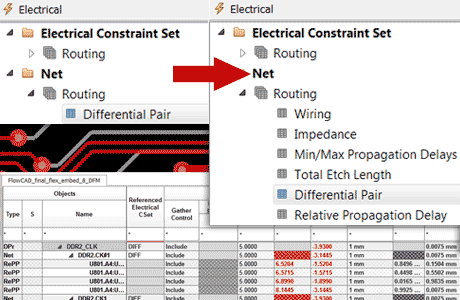
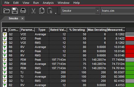
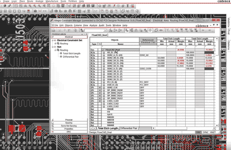
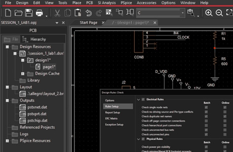
OrCAD PCB Designer Professional with PSpice is a PCB design software for most of the designs developed today. The PCB software already has the circuit diagram module OrCAD Capture and OrCAD PCB Editor with integrated Constraint Manager. The scalable OrCAD / Allegro PCB platform provides investment protection for the user, as increasing technical requirements based on the same data base can be used to upgrade to more powerful Allegro licenses. Several design rule checks are performed in real time to help the designer implement the design intent and follow all design rules. It includes a full version of PSpice A/D and Smoke option for reliability analysis.

Product Features

OrCAD Capture
Schematic Entry OrCAD Capture

Schematic Entry with OrCAD Capture

OrCAD Capture schematic entry tool for circuit diagrams is one of the world's most widely used software for entering and documenting electrical circuits. OrCAD Capture uses flat or hierarchical schematics. Via the navigation window the different pages of the schematic can be selected and thematically managed according to functional blocks. By using the integrated interface, it is also possible to use parts from Ultra Librarian and SamacSys, which offer millions of components. The electrical connections between the component pins can be established quickly and rules can already be defined on schematic level.
Learn More

PCB Editor
PCB Editor

PCB Editor for Physical Layout

PCB Editor is the canvas to perform PCB layout. With many automated functions the designer can efficiently implement the physical design with traces, planes, component footprints, drill holes, etc. While working with automated assistance, design rule checks in real time help to follow design rules and implement the design intent ready for PCB production quickly. Interactively working in 2D and 3D offers advantages depending on the task.

SPECCTRA auto router

SPECCTRA auto router

The SPECCTRA auto router can help to complete the routing of a PCB without a limit in layers. To influence the layout several parameters can be adjusted, such as fanout and routing direction. The auto router in OrCAD Professional also takes high speed rules like propagation delay into account. A router might not do the complete board, but when used wisely it supports the PCB designer to finish digital elements with constraints faster. Feasibility studies are done in minutes and give an indication, if the board is routable with this number of layers. Auto-interactive routing commands support the user in manipulation the automatically done routing.

OrCAD Scalability
OrCAD Scalability

OrCAD Scalability

OrCAD PCB Designer is based on Allegro PCB design technology and both (OrCAD and Allegro) use the same design database. The difference in the licenses is the feature set how to automatically edit and verify the design. The number of design rule checks varies by the type of license. The big advantage is, that you only pay for the functionality you need. When working in a team with multiple licenses, you can check out and use the license you need to perform a certain task or check. All information is stored in the same database.

Online Design Rule Check DRC
DRC Error

Online Design Rule Check DRC and DFM Checks

During routing, the tool checks whether design rules are violated in real-time. When errors are caused, e.g. by placing a component in an unauthorized location, the tool will highlight a design rule violation. All rules defined in Constraint Manager can be checked. Unique for PCB layout tools are the more than 250 integrated DFM checks, which check against specifications of the PCB fabricator, assembly service provider or test facility, by automatically reading in their rules sets.

Constraint Manager
Constraint Manager

Constraint Manager

The central Constraint Manager makes it easy to define design rules and assign topologies. The rules are hierarchically defined and can be assigned to a number of nets at the same time. With design rule sets as constraint sets (CSet), several rules can be summarized and reapplied in subsequent designs. Physical, spacing and DFM rules are spported but also electrical rules for high speed signals like impedances, min/max length and numbers of vias. more

SI Simulation
SI Simulation

Signal Integrity (SI) Simulation

Clicking on a net in the schematic can open the simulation for signal integrity. By changing the length or impedance, the signal quality can be analysed. IBIS models can be used for driver and receiver components when available, otherwise Cadence default models can be used with parameters from the datasheet. You can extract routed layouts and, i.e., simulate crosstalk of coupled lines. By swapping drivers you can test robustness of the layout for placement alternatives.

Electrical Rules Check

Electrical Rules Check (ERC)

Based on the geometry of routing and stackup of the printed circuit board an electrical rule check can be performed without any simulation models. Impedance discontinuities and coupling of parallel traces are discovered and can be assessed in table form or highlighted with a color overlay directly in PCB Editor canvas. This helps the designer to identify critical hotspots in minutes with no extra setup.

High-Speed Constraints

High-Speed Constraints

High-speed signals have to follow the design rules for transmission lines. This extra set of design rules can be defined in the Constraint Manager and will be verified during PCB layout by real time design rule checks. These DRCs cover parameters like: impedance, min / max length, differential impedance, matched length for groups of nets, routing layers, diff pair necking, and more.

OrCAD PCB Flow Integration

PSpice for Reliability Simulation

OrCAD PCB Designer Professional includes a full version of PSpice A/D incl. Smoke option. With this feature set you can perform a stress analysis of components and ensure you have components reliability as needed. Maximum de-rating of components can be determined and thus make a statement about the component load. The load can be specified in percent via model parameters. The developer is interested in statements about the types of load: thermal at maximum current and highest possible voltage, conduction of junction temperature in °C or thermal contact resistances jC and jA, as they occur in the circuit.
PSpice Feature comparison

YouTube Videos

3:02

Why OrCAD

OrCAD Capture is one of the most widely used schematic design solutions for the creation and documentation of electrical circuits. Fast, easy, and intuitive circuit capture, along with highly integrated flows supporting the engineering process, make OrCAD Capture one of the most popular design environments for today’s product creation.

Real-Time Feedback and ECO
1:15

Real-Time Feedback and ECO

Real-time feedback and design synchronization helps keep the data between your CAD tools in check, so you don’t have to manually identify and resolve the errors or differences. As you work on your schematic, enable the online DRC check for any rule to be automatically notified of any issues that occur as you design. Clicking on any of the warnings or errors from the list, immediately takes you to the issue on the canvas. Once you’ve resolved the errors, you can easily compare the data in your schematic versus the data in your PCB editor and see a preview of what has been modified between the designs.

Product Feature Comparison for OrCAD PCB Designer

    OrCAD PCB Designer Standard OrCAD PCB Designer Professional OrCAD PCB Designer Professional with PSpice
OrCAD Capture
PCB Editor
SPECCTRA auto router -
Scalable to Allegro
DFM rules checks 250 250 250
Constraint Manager basic
SI simulation basic
Electrical Rule Check (ERC) -
High-speed DRC -
PSpice simulation basic basic PSpice A/D + Smoke
This table is for information only. For details consult the official datasheets from Cadence.